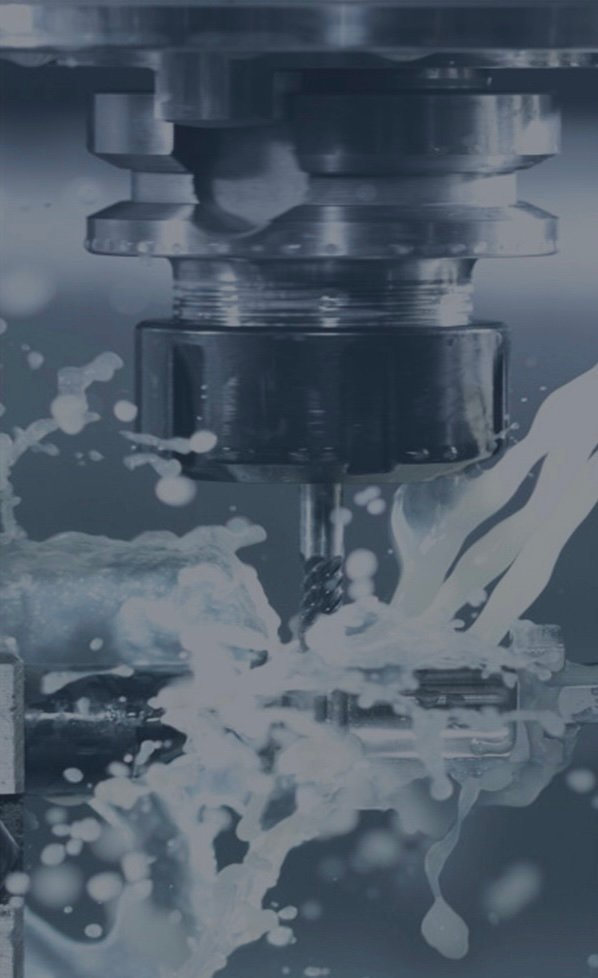

The semiconductor industry operates at the frontier of modern manufacturing, producing chips that power everything from consumer electronics to aerospace systems. As transistor nodes continue to shrink below 5 nm and 3 nm thresholds, the equipment used to fabricate these chips must perform with extraordinary precision and consistency. Even the smallest dimensional deviation in a critical equipment component can cascade into yield losses worth millions of dollars per production run.
CNC Machining for the Semiconductor Industry
CNC machining has established itself as a foundational manufacturing method for producing the high-precision components that semiconductor equipment demands. Its ability to hold micron-level tolerances, machine complex geometries, and deliver consistent results across production volumes makes it uniquely suited to this industry. This article examines how CNC machining contributes to semiconductor equipment performance, component quality, and the broader push toward next-generation chip fabrication technology.
Understanding Semiconductor Equipment Manufacturing
Semiconductor fabrication is a multi-stage process involving hundreds of precisely sequenced steps to transform raw silicon wafers into functional integrated circuits. Each stage depends on equipment that must perform repeatably within extremely tight process windows. The accuracy of the equipment is not secondary to the process; it is the process.
Major Equipment Used in Semiconductor Production
The core equipment categories in a semiconductor fab include:
- Lithography systems: Project circuit patterns onto wafer surfaces using UV or extreme ultraviolet light. Pattern placement accuracy is measured in nanometers, making structural rigidity and thermal stability of the machine frame critical.
- Etching machines: Remove material selectively from wafer surfaces using plasma or chemical processes. Chamber geometry and surface condition directly affect etch uniformity across the wafer.
- Deposition equipment: Deposit thin films of material onto wafers through chemical vapor deposition (CVD) or physical vapor deposition (PVD). Chamber dimensional accuracy governs film thickness uniformity.
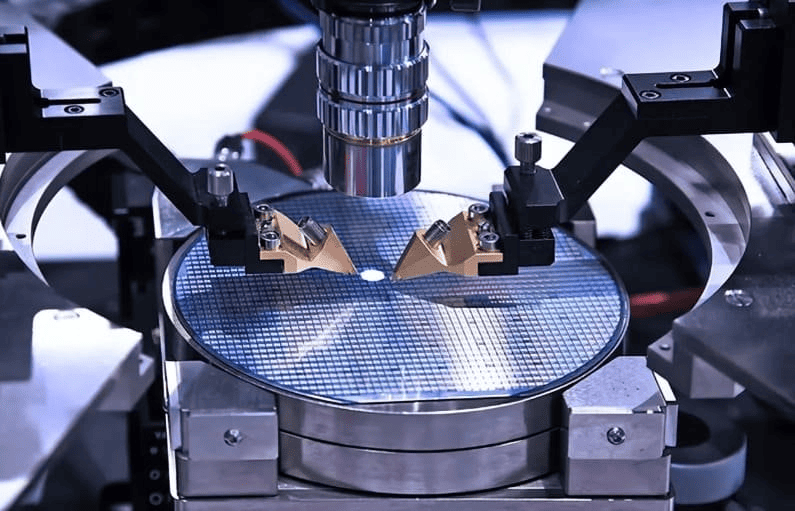
- Wafer handling systems: Transport wafers between process stations without introducing contamination or mechanical stress. Positioning repeatability requirements are typically within a few microns.
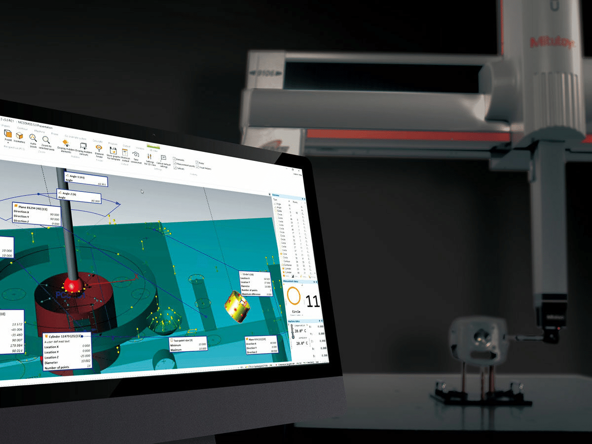
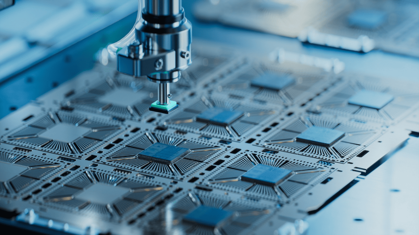
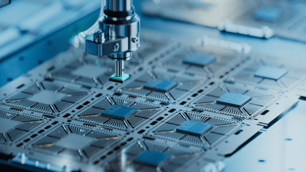
- Inspection and metrology tools: Measure critical dimensions, surface defects, and film properties at multiple points in the process flow. Their own structural components must be dimensionally stable to deliver reliable measurements.
Why Equipment Accuracy Directly Impacts Chip Quality
Every equipment component in a semiconductor fab sits within a chain of interdependent process steps. A dimensional error in a vacuum chamber wall affects pressure uniformity. A misaligned stage affects pattern overlay accuracy. A poorly finished gas delivery component introduces contamination. At advanced nodes, these are not theoretical risks; they are yield-killing realities that fabs work continuously to eliminate. [1]
The Growing Demand for Tighter Tolerances
As semiconductor nodes shrink, the tolerance requirements placed on equipment components tighten in parallel. A component acceptable for 28 nm production may be entirely unsuitable for 3 nm fabrication. EUV lithography machines, for example, require optical and structural components machined to tolerances measured in tens of nanometers, with surface finishes and thermal stability specifications that push conventional machining to its limits. ASML, the sole manufacturer of EUV systems, sources components machined to sub-micron tolerances from a highly specialized supply chain. This trend toward tighter specifications is not temporary; it is the defining trajectory of the industry. [2]
Why Precision Is Critical in Semiconductor Equipment
Precision in semiconductor equipment is not a quality preference; it is an operational necessity. The physics of chip fabrication at advanced nodes leaves virtually no margin for dimensional error, misalignment, or surface contamination. Every component in the equipment chain must perform within its specified tolerance consistently, across thousands of operating hours, under the thermal, mechanical, and chemical stresses of a live production environment.
Micron-Level and Sub-Micron Tolerances
At advanced semiconductor nodes, equipment components are routinely specified to tolerances of ±1 µm or tighter. This is not limited to optical components; structural parts, vacuum flanges, stage assemblies, and gas delivery fittings all carry precision requirements that would be considered exceptional in most other industries. Achieving these tolerances in production, rather than in a laboratory setting, requires machines with high geometric accuracy, stable thermal environments, and rigorous process control throughout the machining workflow. [3]
Impact of Dimensional Errors on Production
Dimensional errors in semiconductor equipment propagate directly into wafer-level defects:
- Pattern overlay errors: A wafer stage that is out of position by even 10 nm causes misalignment between successive lithography layers, producing non-functional devices.
- Film non-uniformity: Deposition chamber components with incorrect geometry alter gas flow distribution, resulting in films of uneven thickness across the wafer surface.
- Etch non-uniformity: Plasma etch chambers with dimensional deviations from design produce inconsistent etch rates across the wafer, reducing die yield.
- Particle contamination: Poorly finished internal surfaces in vacuum chambers or gas lines shed particles that land on wafer surfaces, creating defects that cannot be corrected downstream.
Each of these failure modes translates directly into reduced yield, which in high-volume semiconductor manufacturing represents substantial financial loss per affected lot. [4]
Vibration Control and Alignment Accuracy
Semiconductor equipment operates in environments where vibration must be actively controlled. Lithography systems, in particular, use active vibration isolation platforms to decouple the optical column from floor vibration. The machined components that form these platforms and support structures must be geometrically accurate and properly balanced to avoid introducing their own vibration sources. Alignment accuracy of optical and mechanical assemblies depends on the precision of the machined mounting surfaces and reference features that locate each component within the system. Even minor surface flatness errors on a mounting face can introduce angular misalignment that degrades imaging performance across the entire wafer field.
Surface Finish Requirements for Contamination-Sensitive Environments
Inside a semiconductor process tool, surface finish is a contamination control parameter, not merely an aesthetic one. Rough internal surfaces in vacuum chambers trap process gases, outgas under vacuum, and shed particulates. Electropolished or precisely machined surfaces with low Ra values reduce these risks significantly. For components exposed to aggressive chemistries such as fluorine-based etch gases, surface finish also affects chemical resistance, as rougher surfaces present a higher effective surface area for chemical attack, accelerating corrosion and particle generation. [5]
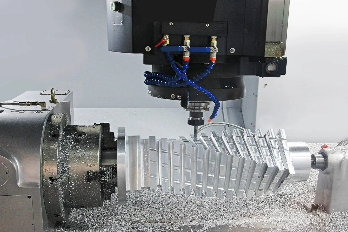
CNC Machining Technologies Used in Semiconductor Manufacturing
No single CNC process covers the full range of components required in semiconductor equipment. The diversity of part geometries, materials, and tolerance requirements across a single machine tool demands an equally diverse set of machining technologies. In practice, semiconductor equipment manufacturers and their supply chains deploy several CNC processes, often in combination, to produce components that meet the industry's exacting standards.
Semiconductor CNC Machining for High-Performance Components
CNC Milling for Complex Geometries
CNC milling is the dominant process for producing the structural and functional components that define semiconductor equipment architecture. Vacuum chamber bodies, equipment frames, mounting plates, and gas manifolds are all primarily milled components. Modern CNC machining centers used in this sector operate with positioning accuracies of ±1 µm or better, supported by thermally compensated machine structures and high-resolution linear encoders.
Key capabilities relevant to semiconductor equipment include:
- Tight flatness and parallelism control on sealing surfaces and mounting faces, where deviations of more than a few microns can compromise vacuum integrity or component alignment.
- Deep pocket and thin-wall machining for lightweight structural components, requiring carefully managed cutting forces to avoid workpiece deflection.
- Complex internal geometries for gas distribution manifolds and cooling channels, where flow path dimensions directly affect process uniformity.
CNC Turning for Cylindrical and Rotational Components
CNC turning produces the cylindrical components found throughout semiconductor equipment: shafts, spindles, fittings, flanges, and rotational stage elements. In this context, turning operations must hold diameter tolerances and surface finishes comparable to those required in aerospace shaft production. Bearing seats on wafer handling spindles, for example, are typically specified to ISO tolerance grades of IT5 or IT6, with surface finish requirements of Ra 0.4 µm or better to ensure proper bearing seating and long service life.
Multi-Axis CNC Machining for Intricate Designs
Five-axis and multi-axis CNC machining has become essential for semiconductor equipment components that combine complex external geometries with internal features requiring access from multiple angles. A five-axis machining center can produce a complex vacuum chamber component, complete with port flanges, internal cooling channels, and precision sealing surfaces, in a single setup. This eliminates the repositioning errors that accumulate when the same part is produced across multiple setups on simpler machines, directly improving the geometric accuracy of the finished component. For semiconductor equipment, where the relationship between multiple features on a single part is often as critical as the features themselves, single-setup machining is a significant quality advantage. [6]
Precision Drilling and Boring Operations
Precision holes in semiconductor equipment components serve as alignment features, fastener locations, vacuum ports, and fluid passages. Requirements for these features extend beyond simple diameter tolerance:
- Position accuracy: Bolt hole patterns on vacuum flanges must align with mating components to within fractions of a millimeter to ensure proper sealing under vacuum.
- Cylindricity: Bored holes used as bearing or bushing seats must be round and straight throughout their depth, not merely correct in diameter at a single cross-section.
- Surface finish in bored holes: Internal surfaces of precision bores are often specified to Ra 0.8 µm or better, particularly where they serve as running surfaces or sealing interfaces.
Jig boring and precision CNC boring operations using single-point boring bars achieve these requirements routinely in semiconductor equipment production.
High-Speed Machining for Advanced Materials
Several materials common in semiconductor equipment, including aluminum alloys, titanium, and engineering ceramics, are best processed using high-speed machining strategies. High spindle speeds combined with light depths of cut and high feed rates reduce cutting forces, minimize heat generation in the workpiece, and produce excellent surface finishes. For aluminum vacuum chamber components, high-speed machining produces the combination of dimensional accuracy and surface quality required without the residual stress and thermal distortion that can result from conventional cutting parameters. [7]
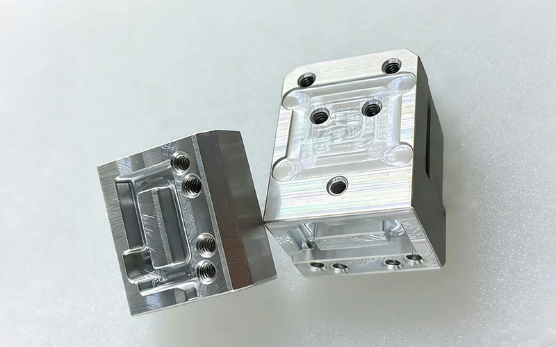
Key Semiconductor Equipment Components Produced by CNC Machining
Semiconductor equipment is an assembly of highly specialized components, each carrying precise dimensional and surface requirements. CNC machining is the primary production method for the majority of these components, spanning structural assemblies, process-critical chambers, and precision motion systems. Understanding what each component demands from the machining process clarifies why conventional manufacturing methods are insufficient in this industry.
Vacuum Chambers
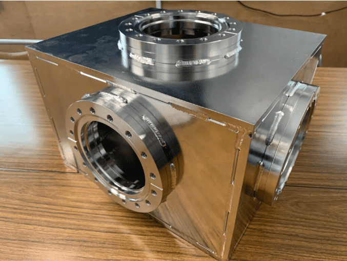
Vacuum chamber for semiconductor equipment
Vacuum chambers are among the most dimensionally demanding components in semiconductor equipment. They must maintain structural integrity under atmospheric pressure loading while holding internal geometry accurate enough to support uniform process conditions across the wafer surface. CNC machining requirements for vacuum chambers include:
- Flatness on sealing surfaces: Conflat and ISO flanges require sealing face flatness within a few microns to achieve leak-tight metal or elastomer seals under high or ultra-high vacuum conditions.
- Internal surface finish: Electropolished or precisely machined internal surfaces minimize outgassing and particle generation, both of which degrade process performance in deposition and etch applications.
- Port and feature positioning: Vacuum ports, viewport flanges, and instrumentation feedthroughs must be positioned accurately relative to the chamber centerline to align with external hardware and process tooling.
Aluminum alloy chambers, particularly those machined from 6061-T6 or 6063 stock, dominate in CVD and PVD applications due to the material's combination of machinability, low outgassing, and compatibility with anodizing treatments that improve surface durability. [8]
Wafer Stages and Positioning Systems
Wafer stages are the motion-critical components that position the wafer relative to the process or imaging system with nanometer-level repeatability. The machined components within a wafer stage include:
- Stage bodies and carriages: Machined from granite, aluminum, or low-expansion alloys to combine structural stiffness with minimal thermal growth. Surface flatness on bearing and guideway mounting surfaces is critical to stage straightness and repeatability.
- Linear guideway seats: The surfaces on which precision linear guides are mounted must be flat and parallel to within microns across the full travel length of the stage, as any deviation directly appears as positioning error during wafer scanning.
- Encoder scale mounting features: Position encoder scales must be mounted on accurately machined reference surfaces to ensure that the measured position corresponds to the actual stage position throughout the travel range.
A misaligned wafer stage introduces overlay errors between successive lithography exposures, which at advanced nodes below 10 nm can render entire wafer lots non-functional. The cost of such yield loss makes the precision of stage component machining a direct financial variable in fab economics.
Equipment Frames and Structural Assemblies
The structural frame of a semiconductor process tool provides the geometric reference for every component mounted within it. Frame accuracy determines the alignment of process modules, optical columns, and handling systems relative to one another. CNC machining requirements for structural assemblies include:
- Datum surface accuracy: Primary reference surfaces must be machined flat and square to serve as reliable mounting references throughout the equipment assembly process.
- Hole pattern accuracy: Precision-drilled and bored hole patterns locate sub-assemblies and modules within the frame. Positional errors in these patterns translate directly into misalignment of the mounted components.
- Residual stress management: Large structural components machined from aluminum or steel plate can retain residual stresses from the rolling or casting process. These stresses relax over time, causing dimensional drift. Proper material selection, pre-machining stress relief, and conservative material removal strategies are necessary to produce stable frames. [9]
Precision Brackets and Mounting Fixtures
Brackets and mounting fixtures locate sensors, optical components, gas injectors, and other functional elements within the process environment. Though individually smaller than chambers or frames, these components often carry the tightest relative tolerance requirements in the assembly, as they directly govern the position of process-critical items. A sensor bracket that is 50 µm out of position can cause a wafer inspection system to miss defects or generate false readings, neither of which is acceptable in production.
Gas Delivery System Components
Gas delivery components, including manifolds, injectors, and distribution blocks, control the flow of process gases into etch and deposition chambers. CNC machining requirements for these parts focus on:
- Internal passage geometry: Flow path cross-sections and lengths must be accurate to ensure designed flow rates and pressure drops are achieved in service.
- Surface finish on wetted surfaces: Internal surfaces exposed to reactive process gases must be smooth and free of machining marks that trap gas, promote corrosion, or generate particles.
- Port and fitting interfaces: Threaded or flanged connection points must be accurately positioned and dimensioned to mate correctly with upstream and downstream plumbing. [10]
Cooling Plates and Thermal Management Parts
Thermal management is a critical engineering challenge in semiconductor equipment, where process heat must be removed efficiently to maintain dimensional stability and protect sensitive components. CNC-machined cooling plates incorporate:
- Internal cooling channels: Milled or drilled passages carry temperature-controlled fluid through the component. Channel geometry, including cross-section, spacing, and path length, governs thermal uniformity across the plate surface.
- Surface flatness: Cooling plates that interface with process components or wafer chucks must be flat to ensure uniform thermal contact and consistent temperature distribution across the wafer.
- Material selection: Aluminum is the dominant material for cooling plates due to its high thermal conductivity and machinability, while stainless steel is used where chemical compatibility with cooling fluids is required.
Conclusion
CNC machining is the technical foundation on which semiconductor equipment performance is built. Every component category covered in this article, from vacuum chambers to wafer stages to cooling plates, depends on it to achieve the dimensional accuracy and surface integrity that advanced fabrication demands.
As chip nodes shrink and process windows narrow, the precision requirements placed on machined components will only intensify. CNC machining, supported by continuing advances in machine accuracy and process control, remains the most capable and scalable method for meeting those requirements, and its role in the semiconductor supply chain is deepening alongside the industry it serves.
References
Allwood, J. M., Childs, T. H., Clare, A. T., De Silva, A. K., Dhokia, V., Hutchings, I. M., Leach, R. K., Leal-Ayala, D. R., Lowth, S., Majewski, C. E., Marzano, A., Mehnen, J., Nassehi, A., Ozturk, E., Raffles, M. H., Roy, R., Shyha, I., & Turner, S. (2015). Manufacturing at double the speed. Journal of Materials Processing Technology, 229, 729–757. https://doi.org/10.1016/j.jmatprotec.2015.10.028
Arun, A. P., Sreenivasan, N., Patil, J. H., Kusanur, R., Ramachandraiah, H. L., & Ramakrishna, M. (2025). Thin Films for Next Generation Technologies: A comprehensive review of fundamentals, growth, deposition strategies, applications, and emerging frontiers. Processes, 13(12), 3846. https://doi.org/10.3390/pr13123846
Cao, D., Dong, H., Zeng, Z., Zhang, W., Li, X., & Yu, H. (2025). Thermal Control Systems in Projection Lithography Tools: A Comprehensive review. Micromachines, 16(8), 880. https://doi.org/10.3390/mi16080880
Chen, H., & Chen, C. (2025). Reviews of the static, adoptive, and dynamic sampling in wafer manufacturing. Applied System Innovation, 9(1), 1. https://doi.org/10.3390/asi9010001
Dahmen, T. (2021). Additive Manufacturing for Fuel Injectors: Design, Processes and Materials. DTU Mechanical Engineering. https://doi.org/10.13140/rg.2.2.21672.85762
Fragassa, C., Vetricini, J., Latini, M., Merlin, M., & Santulli, C. (2026). Experimental investigation of surface contamination removal in machined metals using Multi-Technique characterization. Metals, 16(5), 485. https://doi.org/10.3390/met16050485
Krimpenis, A. A., & Iordanidis, D. M. (2023). Design and analysis of a desktop Multi-Axis Hybrid Milling-Filament Extrusion CNC machine tool for Non-Metallic materials. Machines, 11(6), 637. https://doi.org/10.3390/machines11060637
Möhring, H., Biermann, D., Bleicher, F., Melkote, S., & Kappmeyer, G. (2025). Fixtures and workpiece clamping systems in machining. CIRP Annals, 74(2), 945–969. https://doi.org/10.1016/j.cirp.2025.04.096
Orji, N. G., Badaroglu, M., Barnes, B. M., Beitia, C., Bunday, B. D., Celano, U., Kline, R. J., Neisser, M., Obeng, Y., & Vladar, A. E. (2018). Metrology for the next generation of semiconductor devices. Nature Electronics, 1(10), 532–547. https://doi.org/10.1038/s41928-018-0150-9
Sambo, A. M., Younas, M., & Njuguna, J. (2024). Insights into Machining Techniques for Additively Manufactured Ti6Al4V Alloy: A Comprehensive Review. Applied Sciences, 14(22), 10340. https://doi.org/10.3390/app142210340