
Technology in the semiconductor industry is constantly developing because consumers want more powerful gadgets that can do more. Next-generation processes in the semiconductor industry necessitate high levels of accuracy, dependability, and cleanliness.
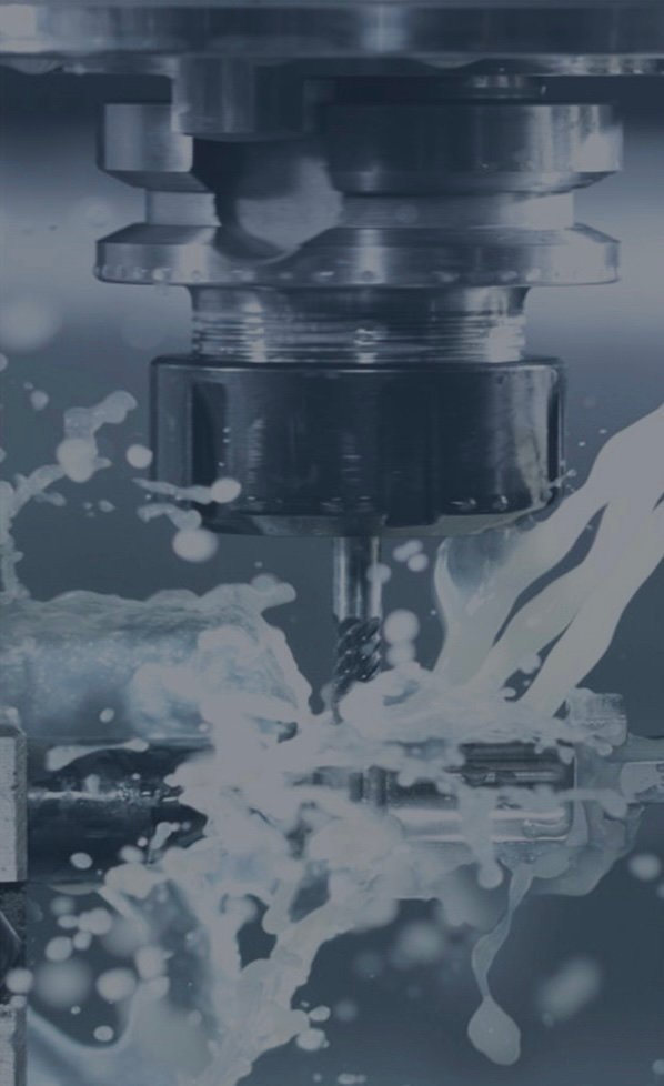
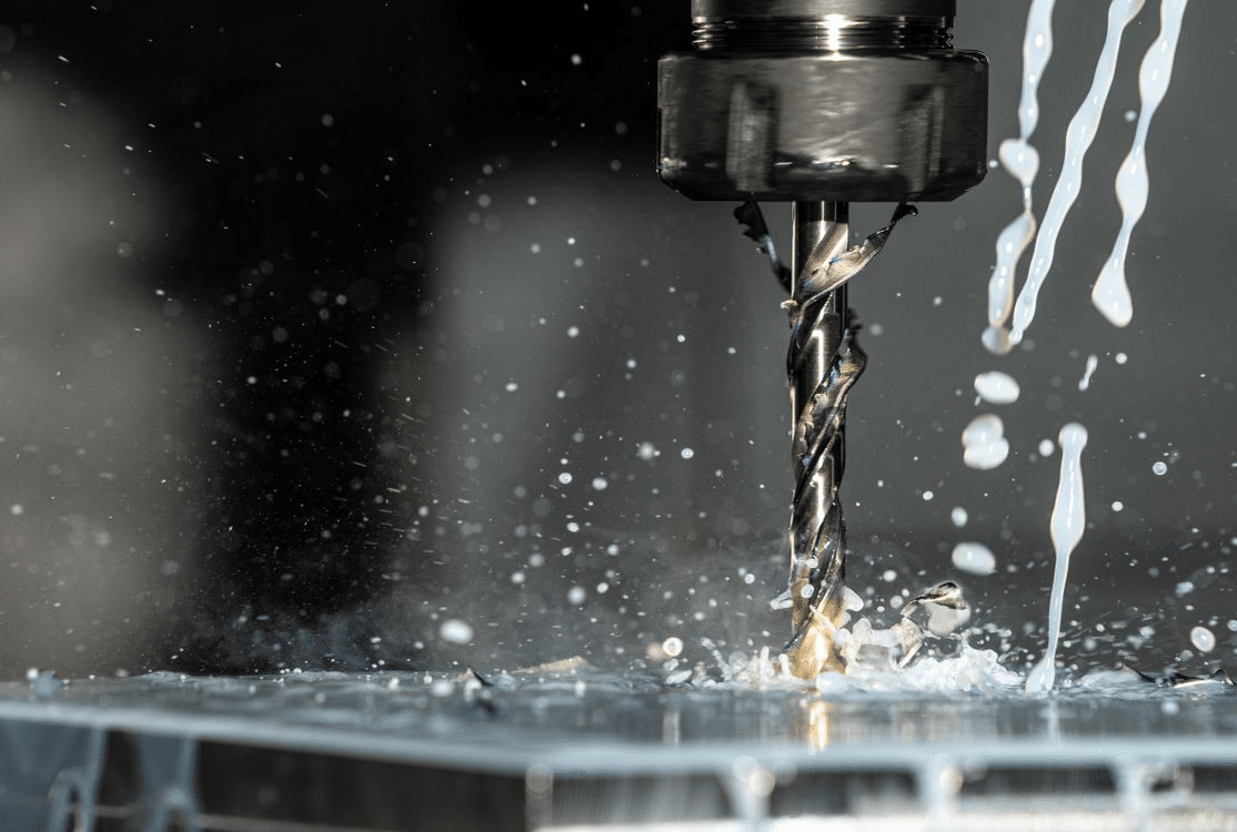
The technology behind vacuum chambers is important to meeting these criteria, as it is responsible for producing the conditions required for semiconductor production. Vacuum chambers are vital in the completion of crucial procedures, including deposition, etching, and implantation, by providing controlled settings with low-pressure conditions.
This piece goes into detail about the benefits and problems of using vacuum chambers in the next generation of semiconductor manufacturing. It shows how important they are and what strategies are used to meet the changing needs of the industry.
Vacuum Chamber Technology in Semiconductor Manufacturing - Overview
Vacuum technology plays a vital role in the semiconductor manufacturing industry by ensuring clean and controlled conditions during the production of advanced silicon chips. This enables the production of smaller and faster components used in modern electronics.
Source
Within semiconductor manufacturing, vacuum chambers are essential to creating the appropriate environment for conducting various processes such as chemical vapor deposition, etching, and sputtering. The table below outlines some of these processes and their corresponding details while illustrating their role in semiconductor manufacturing.
| Process | Description |
| Chemical Vapor Deposition | It involves introducing reaction gases into the chamber to form thin films on substrate surfaces for device fabrication |
| PVD (Sputter Deposition) | Sputter deposition occurs when ions hit a target material and break its bonds producing neutral atoms that then deposit onto a substrate surface |
| Plasma Etching | A type of dry etching process that involves exposing the material to reactive plasma environments to remove layers selectively |
Moreover, vacuum technology offers advantages like lower costs by allowing continuous processing due to its dust-free environment, reducing contamination that can harm equipment performance.
Pro Tip: It is crucial to maintain cleanliness standards for an efficient operating environment within any vacuum-based system involved in chip production.
Without vacuum chambers, the semiconductor industry would be as reliable as a cheap vacuum cleaner.
Importance of Vacuum Chambers in Semiconductor Manufacturing
Semiconductor manufacturing relies heavily on the application of vacuum technology. This is essential for the creation of high-quality and reliable semiconductor devices by removing contaminants, reducing mechanical stress, and providing a controlled environment.
| Benefits | Functionality | Examples |
| Contamination control | Removal of gas molecules, dust particles, and other contaminants | Vacuum deposition systems, electron beam lithography systems, and ion implantation machines |
| Mechanical stress reduction | Elimination of air pressure that can cause strain on fabricated components | CVD systems employing low-pressure plasma processes, PECVD machines, and advanced dry-etching equipment. |
Vacuum chamber technology is not only important for the current generation but also plays a significant role in shaping the next generation for semiconductor manufacturing. Innovations in vacuum chamber technology are always ongoing to ensure they meet the latest demands from the semiconductor industry.
One fascinating historical aspect to note about vacuum chambers involves Robert Boyle. He was one of the early pioneers to conduct experiments around vacuum technology in the seventeenth century which has helped shape its use today.
With all these different types of vacuum chambers, semiconductor manufacturing is starting to sound like a sci-fi movie set.
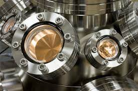
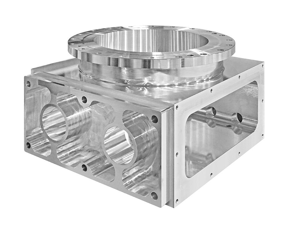
Different Types of Vacuum Chambers Used in Semiconductor Manufacturing
Vacuum chambers are crucial in semiconductor manufacturing for a myriad of reasons. Here, we will explore the various types of vacuum chambers employed in semiconductor manufacturing and their applications.
| Chamber Type | Description | Application |
| Evaporator Chamber | Used for thin film deposition through vaporization of solid materials. | For making thin films on wafers or other substrates. |
| Sputtering Chamber | Utilizes plasma to generate ions that dislodge material from the target, depositing it onto the substrate. | For deposition of metals and insulators. |
| Annealing Chamber | Used to heat samples under vacuum conditions to activate dopants or repair crystal structure defects. | For post-processing heat treatment of samples in a compressed environment with minimal contamination. |
The types mentioned in the table are not exhaustive but provide insight into some commonly used vacuum chambers used in different manufacturing steps. Each chamber plays a unique role and can be optimized for specific manufacturing requirements.
Collisions between gas molecules inside vacuum tanks often cause unwanted particle movement, resulting in contamination. However, careful selection of materials used within a chamber as well as its operational conditions, e.g., pressure levels, can minimize such effects.
Source
https://vacgen.com/all-products/chambers
We recommend regular maintenance checks that include cleaning and inspection of each component within your vacuum chamber system. Replace worn-out parts to prevent leaks and optimize operational efficiency. This approach ensures overall equipment effectiveness, improves sample quality, and reduces equipment downtime.
Choosing the right vacuum chamber for semiconductor manufacturing is like choosing a life partner - it's all about finding the perfect fit.
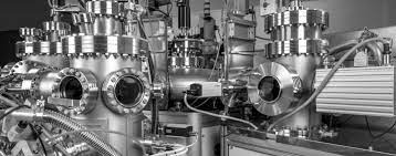
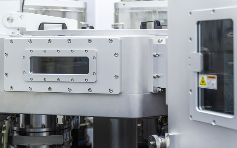
Key Components of a Vacuum Chamber
The contamination of modern semiconductor processes is a significant problem. The performance and yield of a device can be negatively impacted by even the smallest particles, trace gases, or outgassing from chamber materials.
In order to keep vacuum chambers ultra-clean, it is necessary to use efficient contamination management measures to reduce particle formation, regulate outgassing, and prevent contamination.
Take a closer look at these components:
Vacuum Pumps
The vacuum pump is the central component of any vacuum system. They have to get rid of the air and other gases in the chamber to get the pressure down to where it needs to be. In order to achieve the desired vacuum level and pumping speed, various vacuum pump types are employed.
Some common types are rotary vane pumps, turbomolecular pumps, cold pumps, and ion pumps. Choosing the right vacuum pump relies on things like the ultimate vacuum level, the required pumping speed, the compatibility of the gases, and the control of contamination.
Pressure Measurement and Control Systems
Maintaining the proper vacuum level inside the chamber requires precise pressure measurement and management. Gauges and transducers are used to measure and track the pressure inside the container. Mechanical, thermal, and ionization-based data are only some of the possible foundations for these instruments.
Valves and regulators make up pressure control systems, which help keep the pressure steady by regulating gas flow or releasing pressure buildup. These controls allow for instantaneous adjustments to be made in response to changing conditions in the process.
Sealing Mechanisms
Maintaining the vacuum chamber's integrity and preventing air or gas leakage requires reliable sealing mechanisms. Different methods of sealing are used for different chamber configurations and functions. Elastomeric O-rings, metal gaskets, and knife-edge seals are all examples of common sealing mechanisms. In order to keep contaminants out and vacuum in, the seals need to be hermetically tight despite the pressure differences.
Gas Handling Systems
Gas handling systems are necessary for putting and controlling process gases inside the vacuum room. Components of these systems include gas supply lines, injection mechanisms, and mass flow controllers. In order to maintain stable conditions throughout a process, mass flow controllers are used to regulate the amount of gas being pumped through the system. The distribution and introduction of gases into the chamber through the use of gas delivery lines and injection devices enable regulated reactions and operations.
Technical Specifications for Vacuums in Vacuum Chambers
In order to provide the appropriate process results, next-generation semiconductor processes frequently need to operate at certain vacuum levels. The materials and stage of the process will determine the optimal vacuum level. Important features needed in a vacuum are:
- High-vacuum and ultra-high-vacuum (UHV) conditions: When it comes to minimizing gas-phase reactions, ensuring precise material deposition, and lowering contamination concerns, many cutting-edge procedures require high-vacuum or UHV settings. Vacuum chambers should be able to reach and maintain these pressures.
- Pressure control and stability: The method demands that vacuum chambers have stable pressure at precisely controlled levels. In order to keep the pressure within the specified range and reduce pressure fluctuations, it is necessary to integrate high-performance vacuum pumps with pressure measurement and control systems and gas handling systems.
- Rapid pump-down and venting: Improving process throughput and decreasing cycle times requires reliable pump-down and venting systems. To maximize efficiency, vacuum chambers should allow for rapid evacuation and the gradual introduction of process gases.
Source
https://yaskawa.co.il/en/product/semiconductor-vacuum-applications/
Factors to Consider When Choosing a Vacuum Chamber for Semiconductor Manufacturing
When selecting a vacuum chamber for semiconductor manufacturing, various parameters should be considered. These parameters can include chamber materials, size, pumping speed, ultimate pressure requirements, and process gas compatibility.
| Parameters | Description |
| Chamber Materials | The materials used to construct the chamber, i.e., stainless steel, may be preferable due to its high resistance to corrosion. |
| Size | A larger chamber may be needed for accommodating larger substrates or creating multi-chamber systems. |
| Pumping Speed | The pumping speed should match the expected outgassing rates of the system. Turbo pumps or oil-free pumps may be preferred depending on requirements. |
| Ultimate Pressure Requirements | This will depend on the required level of precision for the particular process being conducted; keeping low levels of residual gas is imperative where necessary. |
| Process Gas Compatibility | Some materials react with certain gases in ways that may not support effective processing and achieving desirable results. Compatibility must therefore be determined. |
Additionally, different types of control mechanisms may have advantages over others when looking at maintenance costs down the line. Overall, optimizing manufacturing capability requires developing a detailed understanding of requirements to get the best results. Who knew that vacuum chambers could suck the boredom out of semiconductor manufacturing?
It's also crucial to ensure that the system as a whole is capable of providing an optimum manufacturing environment by looking at additional factors such as contamination reduction. Understanding equipment capabilities and limitations improve overall throughput efficiency. In consideration of budget restrictions, refurbishing used equipment might mean less costly purchase spend without compromising on quality or performance.
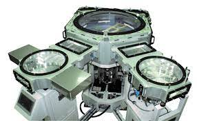
Advancements in Vacuum Chamber Technology for Next-Generation Semiconductor Manufacturing
The latest developments in vacuum chamber technology have been instrumental in enhancing the manufacturing process of next-generation semiconductors. With advanced features such as increased efficiency, higher performance, and greater reliability, the new systems are revolutionizing semiconductor production capabilities.
The advancements in vacuum chamber technology have resulted in several significant improvements. The new chambers provide superior vacuum pressure levels, controlled gas flows, and advanced temperature regulation capabilities. Furthermore, they offer enhanced processing speed and can accommodate larger wafers with increased accuracy.
It is worth noting that these advances go beyond just new equipment upgrades. Groundbreaking research has also been conducted to enhance current processes and introduce innovative solutions. For example, scientists are working on eliminating particle contamination through better filtration methods.
Source
A semiconductor company recently implemented the latest vacuum chamber technology and recorded a 20% increase in production capacity while reducing production time by nearly 50%. They were able to achieve this by utilizing the system's ability to withstand higher temperatures without compromising safety or efficiency.
The advancements in vacuum chambers for next-generation semiconductor manufacturing have made the production process more streamlined and efficient than ever before. With ongoing research and development efforts aimed at pushing technological boundaries even further, it is clear that we are on the brink of an exciting era for semiconductor manufacturing.
Vacuum chamber technology: making sure semiconductors stay clean and happy, like a neurotic germaphobe on cleaning duty.
Case Studies Showcasing the Use of Vacuum Chamber Technology in Semiconductor Manufacturing
Vacuum chambers have become an indispensable technology in semiconductor manufacturing. Many industries have utilized this methodology to create innovative products with precision. Let's take a look at some successful case studies that showcase the use of vacuum chamber technology in the semiconductor manufacturing industry.
| Case Study | Description |
| Samsung | Samsung developed a next-generation SSD drive using a high-powered vacuum chamber that reduced magnetic interference. |
| Intel | Intel utilized a vacuum chamber to improve transistor performance by epitaxial growth, resulting in reliable computing power. |
| Toshiba | Toshiba implemented an advanced vacuum-chamber-based lithography approach that allows up to six layers onto its NAND flash memory chips. |
The case studies highlight how designers and engineers understand the importance of the vacuum technology method. They recognize that it can maintain precise environmental conditions, isolation requirements, and process control standards.
A fascinating detail worth mentioning is that the electronic industry has known about the formation of parasitic oxides during device fabrication for quite some time. However, only after utilizing plasma treatments under a suitable vacuum environment did they successfully eliminate the formation of these parasitic oxides.
According to industry experts, vacuum chamber technology offers accuracy and reliability throughout production processes because it contributes to creating complex structures with controllable properties. Its ability to work on remarkable scales and offer reproducibility reassures engineers as they are able to bring their technological breakthroughs to life.
Vacuum chamber technology: making the future brighter, one semiconductor at a time.
Challenges in Next-Generation Semiconductor Processes
Vacuum chamber design has various issues that need to be fixed in order to accommodate next-generation semiconductor manufacturing methods like improved lithography, 3D integration, and the use of innovative materials. Some of these problems are:
Increased process complexity
Vacuum chambers are necessary for next-generation processes because of the numerous steps and complex sequences involved. These chambers need to be able to house a wide variety of process modules and facilitate smooth wafer handling and transportation.
Tighter process control
As device sizes decrease and circuit complexity rises, it is essential that process parameters be well-regulated. The reproducibility and optimization of yields depend on vacuum chambers with finely-grained control over pressure, temperature, gas flow rates, and other factors.
Contamination control
Contamination is a major problem for modern semiconductor processes. Device performance and yield can be negatively affected by even tiny levels of particles, trace gases, or outgassing from chamber materials. Minimizing particle production, controlling outgassing, and keeping ultra-clean surroundings are all essential functions of vacuum chambers that require effective contamination control measures.
Future Prospects and Potential of Vacuum Chamber Technology in Semiconductor Manufacturing
Vacuum chamber technology revolutionizes semiconductor manufacturing.
As the semiconductor industry demands higher performance and lower costs, vacuum chamber technology has emerged as a critical enabler for achieving these goals. With its ability to create ultra-high vacuum environments that are free from contaminants and particles, vacuum chamber technology offers a range of benefits that enhance the yield, quality, and scalability of semiconductor processes. From lithography and deposition to etching and cleaning, vacuum chambers play a vital role in shaping the future of chip production.
Future prospects and potential of vacuum chamber technology in semiconductor manufacturing
The below table summarizes some of the key trends and opportunities associated with vacuum chamber technology in semiconductor manufacturing.
| Application | Description | Benefit |
| Physical vapor deposition (PVD) | The coating of a solid surface with a thin film by evaporating or sputtering atoms or molecules in a vacuum. | Enhanced adhesion, purity, and uniformity of films. |
| Chemical vapor deposition (CVD) | The creation of a thin film by introducing reactive gases into a heated chamber, where they react to form solid products on surfaces. | Improved conformality, selectivity, and precision of patterns. |
| Lithography | The transfer of a pattern onto a substrate using light, electron beams, or other radiation sources through masks or reticles. | Higher resolution, throughput, and accuracy of masks. |
| Etching | The removal of material from a surface by chemical or physical means using plasma, ion beams, or other techniques. | Better control, uniformity, and selectivity of etch rates. |
| Cleaning | The removal of unwanted residues or particles on wafer surfaces before or after processing using wet or dry methods. | Reduced defects, contamination, and damage to wafers. |
These applications are not mutually exclusive and often combine different vacuum processes in order to optimize the various parameters that affect chip performance, such as electrical conductivity, dielectric strength, thermal resistance, and optical properties.
Vacuum chamber technology also presents some challenges and limitations that require continuous innovation and adaptation. For instance, maintaining ultra-high vacuum conditions can be expensive in terms of energy consumption and equipment complexity.
Ensuring compatibility with different materials and substrates can be difficult due to variations in their chemical and mechanical properties. Controlling the temperature, pressure, flow rate and other process parameters can be intricate because of the multiple interactions between them.
Despite these obstacles, vacuum chamber technology is expected to continue playing a central role in semiconductor manufacturing for years to come. As new materials like carbon nanotubes and graphene emerge as possible replacements for silicon-based chips, the need for precise deposition, etching, and cleaning processes will only grow more pressing.
As new applications like artificial intelligence (AI), Internet-of-Things (IoT), and 5G connectivity drive demand for faster computational speeds at lower power consumption, the need for superior lithography techniques will only increase. As new challenges like climate change, supply chain disruption, and cybersecurity become more urgent, the need for sustainable and resilient manufacturing practices will only intensify.
To stay ahead of these trends and seize the opportunities they offer, both equipment manufacturers and chipmakers should invest in vacuum chamber technology R&D, partnerships and collaborations that exchange knowledge, expertise, and resources. By leveraging each other's strengths and mitigating each other's weaknesses, they can create a virtuous cycle of innovation that benefits everyone in the semiconductor ecosystem.
Don't miss out on this trend - join the vacuum chamber revolution today!
Frequently Asked Questions (FAQs)
What is the role of vacuum pumps in vacuum chamber technology?
Vacuum pumps facilitate the creation of a low-pressure environment in a vacuum chamber by removing gas and other contaminants. They are an essential component of the technology.
How do vacuum chambers prevent contamination in semiconductor manufacturing?
Vacuum chambers use highly controlled conditions to prevent the introduction of contaminants during the creation of semiconductors. By creating a low-pressure environment, the amount of air and particles in the environment is minimized.
How has vacuum chamber technology evolved over time?
Vacuum chamber technology has evolved significantly over time, with advancements in materials, designs, and automation. The next generation of vacuum chambers will have the ability to produce even smaller and more complex chips.
What benefits does vacuum chamber technology offer for semiconductor manufacturing?
Vacuum chamber technology provides a controlled environment for semiconductor manufacturing that leads to consistent quality and production yields. It also enables the production of smaller, faster, and more energy-efficient chips.
Final Words
In conclusion, semiconductor production cannot proceed without vacuum chamber technology. It makes it possible to create the controlled environments that are needed for advanced processes. It also makes sure that the manufacturing process is free of contamination and helps to develop high-performance semiconductor devices. To keep up with the needs of growing semiconductor technologies and to solve new problems, the semiconductor industry will require constant advancements in vacuum chamber technology.